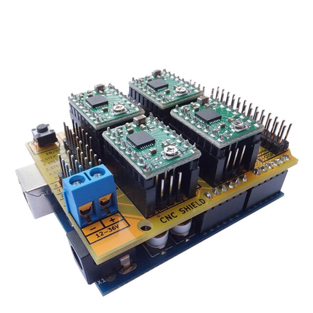
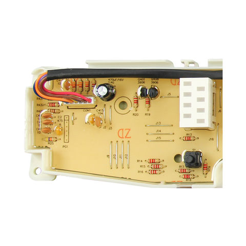
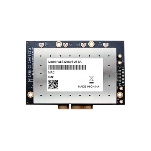
Fire alarm circuit board system board conventional other pcb & pcba
Carbon ink is printed on PCB surface as a conductor to connect two traces on PCB. For carbon ink PCB, the most important is the quality and resistance of carbon oil, meanwhile, the Immersion silver PCB and Immersion tin PCB cannot be printed carbon oil, because they are Oxidizing.Meanwhile, the minimum line space should be more than 0.2 mm so that it is easier to manufacture and control without the short circuit.
Carbon ink can be used for keyboard contacts, LCD contacts and jumpers. The printing is performed with conductive carbon ink.
- Carbon elements must resist soldering or HAL.
- Insulations or Carbon widths may not reduce below 75 % of the nominal value.
- Sometimes a peel able mask is necessary to protect against used fluxes.
Special Carbon Oil Process
- The operator must wear gloves
2.The equipment must be clean, the surface shall not have dust, garbage and other debris
3.Silk speed and back to the ink speed suction pressure control in the best range. (Based on the printing effect as a test)
4.Screen stencil, scraper, carbon oil specific requirements in accordance with the requirements of engineering MI
5.Carbon oil must be mixing evenly before use, with a viscometer to detect the viscosity within the required range, the ink need timely closure after finish the use.
6.Before printing,all boards must be cleaned plate grease, oxide and other pollutants, all carbon plate carbon plate must be confirmed by the QA before the official production
7.Carbon board drying temperature 150 ℃ time 45 minutes. Carbon oil hole Drying temperature 150 ℃ Time 20 minutes
8.Carbon oil resistance measurement, resistance value of carbon oil should be less than 100 ohms, carbon line resistance should be less than 25Ω
9.After the release from oven, the operator should inform the QA to check the carbon resistance and do the adhesion test.
10.Each carbon oil screen version use max 2500 prints, must be returned to the network room re-drying the new version when up to 2500 times.
We believe that Carbon oil PCBA offers an unbeatable combination of quality, performance, and value. If you have any questions about this product or would like to learn more about how it can benefit your business, please don't hesitate to contact us. We are dedicated to providing excellent customer service and helping our customers achieve their business goals.
Thank you for considering Carbon oil PCBA. We look forward to the opportunity to work with you and help you achieve success.
Product Parameters
| Item | Specification |
| Material | FR-4, FR1,FR2; CEM-1, CEM-3,Rogers, Teflon,Arlon,Aluminum Base, Copper Base,Ceramic, Crockery, etc. |
| Remarks | High Tg CCL is Available(Tg>=170℃) |
| Finish Board Thickness | 0.2 mm-6.00mm(8mil-126mil) |
| Surface Finish | Gold finger(>=0.13um), Immersion Gold(0.025-0075um), Plating Gold(0.025-3.0um), HASL(5-20um), OSP(0.2-0.5um) |
| Shape | Routing、Punch、V-cut、Chamfer |
| Surface Treatment | Solder Mask(black, green, white, red, blue, thickness>=12um, Block, BGA) |
| Silkscreen(black, yellow, white) | |
| Peel able-mask(red, blue, thickness>=300um) | |
| Minimum Core | 0.075mm(3mil) |
| Copper Thickness | 1/2 oz min; 12oz max |
| Min Trace Width & Line Spacing | 0.075mm/0.075mm(3mil/3mil) |
| Min Hole Diameter for CNC Drilling | 0.1mm(4mil) |
| Min Hole Diameter for Punching | 0.6mm(35mil) |
| Biggest panel size | 610mm * 508mm |
| Hole Position | +/-0.075mm(3mil) CNC Drilling |
| Conductor Width(W) | +/-0.05mm(2mil) or +/-20% of original |
| Hole Diameter(H) | PTHL:+/-0.075mm(3mil) |
| Non PTHL:+/-0.05mm(2mil) | |
| Outline Tolerance | +/-0.1mm(4mil) CNC Routing |
| Warp & Twist | 0.70% |
| Insulation Resistance | 10Kohm-20Mohm |
| Conductivity | <50ohm |
| Test Voltage | 10-300V |
| Panel Size | 110 x 100mm(min) |
| 660 x 600mm(max) | |
| Layer-layer misregistration | 4 layers:0.15mm(6mil)max |
| 6 layers:0.25mm(10mil)max | |
| Min spacing between hole edge to circuitry pattern of an inner layer | 0.25mm(10mil) |
| Min spacing between board outline to circuitry pattern of an inner layer | 0.25mm(10mil) |
| Board thickness tolerance | 4 layers:+/-0.13mm(5mil) |
Our Advantages
1) Independent R&D capabilities - Our team of experienced software and hardware engineers can design and develop custom electronic boards to fit your specific needs.
2) One-stop service - Our 8 high-speed and 12 high-speed placement machine production lines, as well as 4 plug-in production lines and 3 pipelines, provide a seamless, comprehensive manufacturing process for all our clients.
3) Quick response - We prioritize customer satisfaction and aim to provide quick, efficient service to meet all of your needs.
Products categories
-

Phone
-

E-mail
-

Whatsapp
-

Skype
-

Skype
-

Skype
