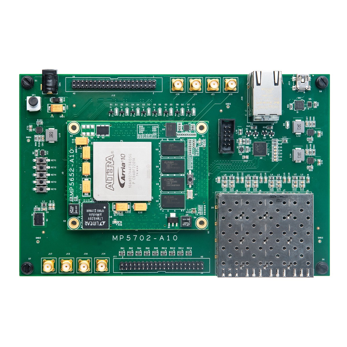
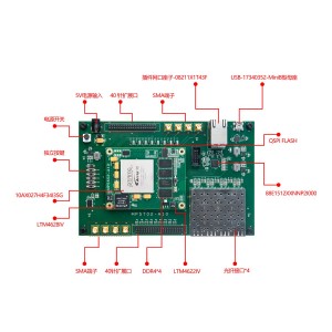
FPGA Intel Arria-10 GX series MP5652-A10
DDR4 SDRAM: 16GBDDR4 Each 16bit composition of the data bit width of the 64bit bit
QSPI Flash: A piece of 1GBQSPIFLASH, which is used to store the configuration file of the FPGA chip
FPGA Bank: adjustable 12V, 18V, 2.5V, 3.0V level, if you need to change the level, you only need to replace
Interface level: The corresponding position can be adjusted by magnetic beads.
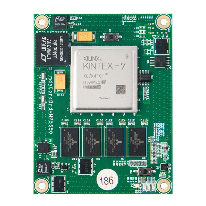
Core board power supply: 5-12V power supply generates two power supply through the T1 chip LTM4628 to meet the FPGA current requirements
Core board startup method: JTAG, QSPIFLASH
Connector tube foot definition: 4 high -speed extensions, 120pin Panasonic AXK5A2137yg
The bottom plate SFP interface: 4 optical modules can achieve high -speed optical fiber communication, with a speed of up to 10GB/s
Fave Plate GXB clock: The bottom plate provides a 200MHz reference clock for the GXB transceiver
The bottom plate 40 -needle extension: reserved 2 2.54mm standard 40 -pin extension J11 and J12, which is used to connect the modules designed by the company or the module function circuit designed by the user themselves
Core plate clock: multiple clock sources on board. This includes 100MHz system clock source
510kba100M000bag CMOS crystal
125MHz Transceiver Differential Clock Sittaid Sit9102 Crystal 300MHz DDR4′s external differential clock source SIT9102 crystal
JTAG debug port: MP5652 core board has a 6PIN patch JTAG download debugging interface
Convenient for users to debug FPGA separately
System reset: At the same time, the button also provides the system with the global reset signal MP5652 core board to support the power -on reset. The entire chip is reset
LED: There are 4 red LED lights on the core board, one of which is DDR4 reference power indicator
Button and switch: There are 4 keys on the bottom plate, which is connected to the corresponding pipe foot on the J2 connector.
Usually high level, pressing to low level
Key features of the Arria-10 GX series include:
- High-density and high-performance logic and DSP resources: The Arria-10 GX FPGAs offer a large number of logic elements (LEs) and digital signal processing (DSP) blocks. This allows for the implementation of complex algorithms and high-performance designs.
- High-speed transceivers: The Arria-10 GX series includes high-speed transceivers that support various protocols such as PCI Express (PCIe), Ethernet, and Interlaken. These transceivers can operate at data rates up to 28 Gbps, enabling high-speed data communication.
- High-speed memory interfaces: The Arria-10 GX FPGAs support various memory interfaces, including DDR4, DDR3, QDR IV, and RLDRAM 3. These interfaces provide high-bandwidth access to external memory devices.
- Integrated ARM Cortex-A9 processor: Some members of the Arria-10 GX series include an integrated dual-core ARM Cortex-A9 processor, which provides a powerful processing subsystem for embedded applications.
- System integration features: The Arria-10 GX FPGAs include various on-chip peripherals and interfaces, such as GPIO, I2C, SPI, UART, and JTAG, to facilitate system integration and communication with other components.
Products categories
-

Phone
-

E-mail
-

Whatsapp
-

Skype
-

Skype
-

Skype


