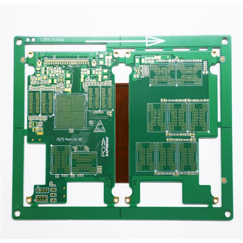
One article understands | What is the basis for the selection of the surface processing process in the PCB factory
The most basic purpose of PCB surface treatment is to ensure good weldability or electrical properties. Because copper in nature tends to exist in the form of oxides in the air, it is unlikely to be maintained as the original copper for a long time, so it needs to be treated with copper.
There are many PCB surface treatment processes. The common items are flat, organic welded protective agents (OSP), full -board nickel -plated gold, Shen Jin, Shenxi, Shenyin, chemical nickel, gold, and electroplating hard gold. Symptom.

- 1. The hot air is flat (spray tin)
The general process of the hot air leveling process is: micro erosion → preheating → coating welding → spray tin → cleaning.
The hot air is flat, also known as hot air welded (commonly known as tin spray), which is the process of coating the melting tin (lead) welded on the PCB surface and using heating to compress the air rectification (blowing) to form a layer of anti -copper oxidation. It can also provide good weldability coating layers. The whole weld and copper of the hot air form a copper -tin metal interductive compound at the combination. PCB is usually sinking in the melting welded water; the wind knife blows the liquid welded flat liquid welded before the welded;
The level of thermal wind is divided into two types: vertical and horizontal. It is generally believed that the horizontal type is better. It is mainly the horizontal hot air rectification layer is relatively uniform, which can achieve automated production.
Advantages: longer storage time; after the PCB is completed, the surface of the copper is completely wet (tin is completely covered before welding); suitable for lead welding; mature process, low cost, suitable for visual inspection and electrical testing
Disadvantages: Not suitable for line binding; due to the problem of surface flatness, there are also limitations on SMT; not suitable for contact switch design. When spraying tin, copper will dissolve, and the board is high temperature. Especially thick or thin plates, tin spray is limited, and the production operation is inconvenient.
- 2, organic weldability protectant (OSP)
The general process is: degreasing --> micro-etching --> pickling --> pure water cleaning --> organic coating --> cleaning, and the process control is relatively easy to show the treatment process.
OSP is a process for printed circuit board (PCB) copper foil surface treatment in accordance with the requirements of the RoHS directive. OSP is short for Organic Solderability Preservatives, also known as organic solderability preservatives, also known as Preflux in English. Simply put, OSP is a chemically grown organic skin film on a clean, bare copper surface. This film has anti-oxidation, heat shock, moisture resistance, to protect the copper surface in the normal environment no longer rust (oxidation or vulcanization, etc.); However, in the subsequent welding high temperature, this protective film must be easily removed by the flux quickly, so that the exposed clean copper surface can be immediately combined with the molten solder in a very short time to become a solid solder joint.
Advantages: The process is simple, the surface is very flat, suitable for lead-free welding and SMT. Easy to rework, convenient production operation, suitable for horizontal line operation. The board is suitable for multiple processing (e.g. OSP+ENIG). Low cost, environmentally friendly.
Disadvantages: the limitation of the number of reflow welding (multiple welding thick, the film will be destroyed, basically 2 times no problem). Not suitable for crimp technology, wire binding. Visual detection and electrical detection are not convenient. N2 gas protection is required for SMT. SMT rework is not suitable. High storage requirements.
- 3, the whole plate plated nickel gold
Plate nickel plating is the PCB surface conductor first plated with a layer of nickel and then plated with a layer of gold, nickel plating is mainly to prevent the diffusion between gold and copper. There are two types of electroplated nickel gold: soft gold plating (pure gold, gold surface does not look bright) and hard gold plating (smooth and hard surface, wear-resistant, containing other elements such as cobalt, gold surface looks brighter). Soft gold is mainly used for chip packaging gold wire; Hard gold is mainly used in non-welded electrical interconnections.
Advantages: Long storage time >12 months. Suitable for contact switch design and gold wire binding. Suitable for electrical testing
Weakness: Higher cost, thicker gold. Electroplated fingers require additional design wire conduction. Because the thickness of gold is not consistent, when applied to welding, it may cause the embrittlement of the solder joint due to too thick gold, affecting the strength. Electroplating surface uniformity problem. Electroplated nickel gold does not cover the edge of the wire. Not suitable for aluminum wire bonding.
- 4. Sink gold
The general process is: pickling cleaning --> micro-corrosion --> preleaching --> activation --> electroless nickel plating --> chemical gold leaching; There are 6 chemical tanks in the process, involving nearly 100 kinds of chemicals, and the process is more complex.
Sinking gold is wrapped in a thick, electrically good nickel gold alloy on the copper surface, which can protect the PCB for a long time; In addition, it also has environmental tolerance that other surface treatment processes do not have. In addition, sinking gold can also prevent the dissolution of copper, which will benefit lead-free assembly.
Advantages: not easy to oxidize, can be stored for a long time, the surface is flat, suitable for welding fine gap pins and components with small solder joints. Preferred PCB board with buttons (such as mobile phone board). Reflow welding can be repeated multiple times without much loss of weldability. It can be used as the base material for COB (Chip On Board) wiring.
Disadvantages: high cost, poor welding strength, because the use of non-electroplated nickel process, easy to have black disk problems. The nickel layer oxidizes over time, and long-term reliability is an issue.
- 5. Sinking tin
Since all current solders are tin-based, the tin layer can be matched to any type of solder. The process of sinking tin can form flat copper-tin metal intermetallic compounds, which makes the sinking tin have the same good solderability as the hot air leveling without the headache flat problem of hot air leveling; The tin plate cannot be stored for too long, and the assembly must be carried out according to the order of the tin sinking.
Advantages: Suitable for horizontal line production. Suitable for fine line processing, suitable for lead-free welding, especially suitable for crimping technology. Very good flatness, suitable for SMT.
Disadvantages: Good storage conditions are required, preferably not more than 6 months, to control tin whisker growth. Not suitable for contact switch design. In the production process, the welding resistance film process is relatively high, otherwise it will cause the welding resistance film to fall off. For multiple welding, N2 gas protection is best. Electrical measurement is also a problem.
- 6. Sinking silver
Silver sinking process is between organic coating and electroless nickel/gold plating, the process is relatively simple and fast; Even when exposed to heat, humidity and pollution, silver is still able to maintain good weldability, but will lose its luster. Silver plating does not have the good physical strength of electroless nickel plating/gold plating because there is no nickel underneath the silver layer.
Advantages: Simple process, suitable for lead-free welding, SMT. Very flat surface, low cost, suitable for very fine lines.
Disadvantages: High storage requirements, easy to pollute. Welding strength is prone to problems (micro-cavity problem). It is easy to have electromigration phenomenon and Javani bite phenomenon of copper under welding resistance film. Electrical measurement is also a problem
- 7, chemical nickel palladium
Compared with the precipitation of gold, there is an extra layer of palladium between nickel and gold, and palladium can prevent the corrosion phenomenon caused by the replacement reaction and make full preparation for the precipitation of gold. Gold is closely coated with palladium, providing a good contact surface.
Advantages: Suitable for lead-free welding. Very flat surface, suitable for SMT. Through holes can also be nickel gold. Long storage time, storage conditions are not harsh. Suitable for electrical testing. Suitable for switch contact design. Suitable for aluminum wire binding, suitable for thick plate, strong resistance to environmental attack.
- 8. Electroplating hard gold
In order to improve the wear resistance of the product, increase the number of insertion and removal and electroplating hard gold.
PCB surface treatment process changes are not very large, it seems to be a relatively distant thing, but it should be noted that long-term slow changes will lead to great changes. In the case of increasing calls for environmental protection, the surface treatment process of PCB will definitely change dramatically in the future.


